Research Areas
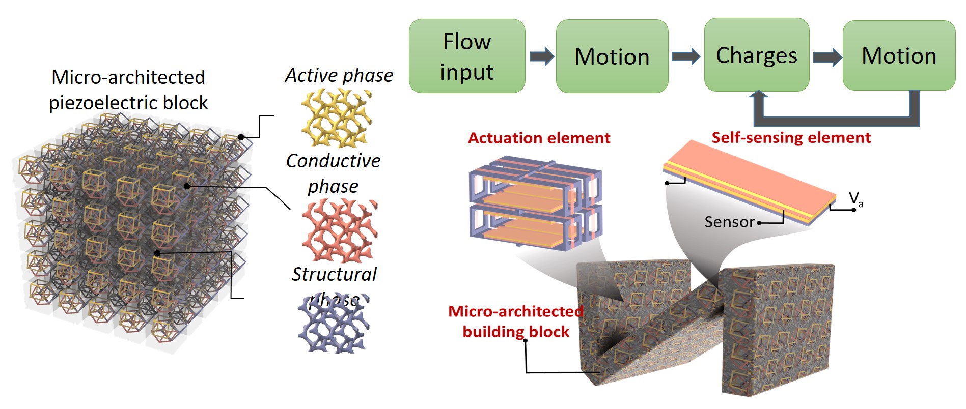
At UC Berkeley, our team focuses on advancing additive manufacturing and processing technologies through innovative techniques that integrate mechanics, optics, and material science. We aim to create multifunctional materials and all-in-one devices with precise 3D architectures for various applications from energy transduction and storage, robotics, health care and structural applications. Our group’s research excellence and translational impact have been recognized through multiple prestigious honors, including the DARPA Young Faculty Award, DARPA Director’s Fellowship for Outstanding Projects, ONR and Air Force Young Investigator Awards, the NSF CAREER Award, as well as Bakar and AIC Awards for entrepreneurship, among others. Beyond research achievements, our group has a strong record of mentorship and academic leadership: more than 40% of our alumni have gone on to secure faculty positions at leading universities. I invite you to visit our research page for a snapshot of our current research activities.
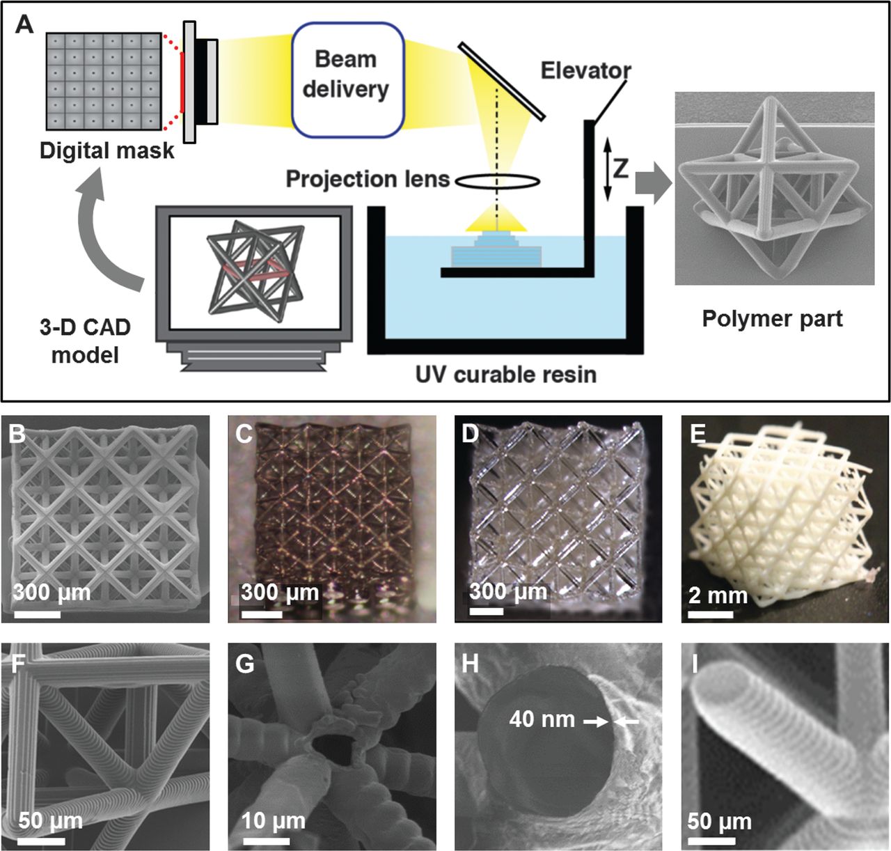
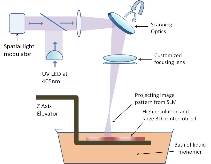
Thrust 1: Additive Manufacturing — Processing Technologies for 3D structures and electronics
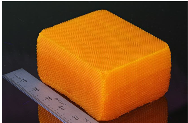
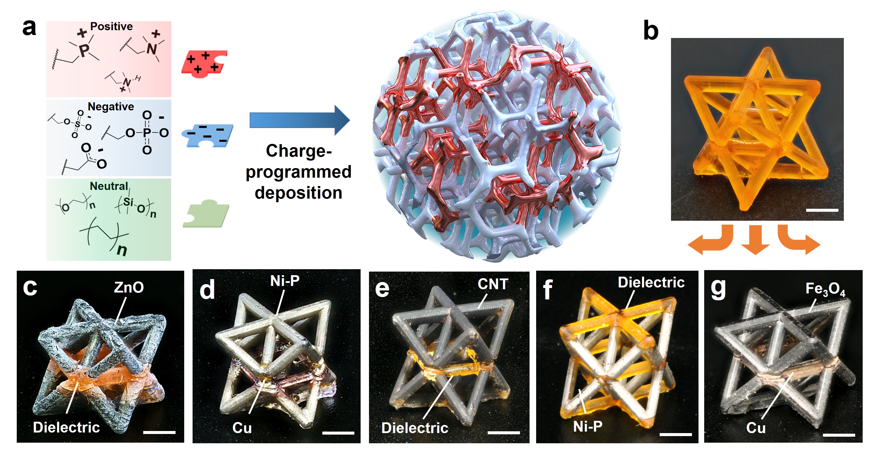
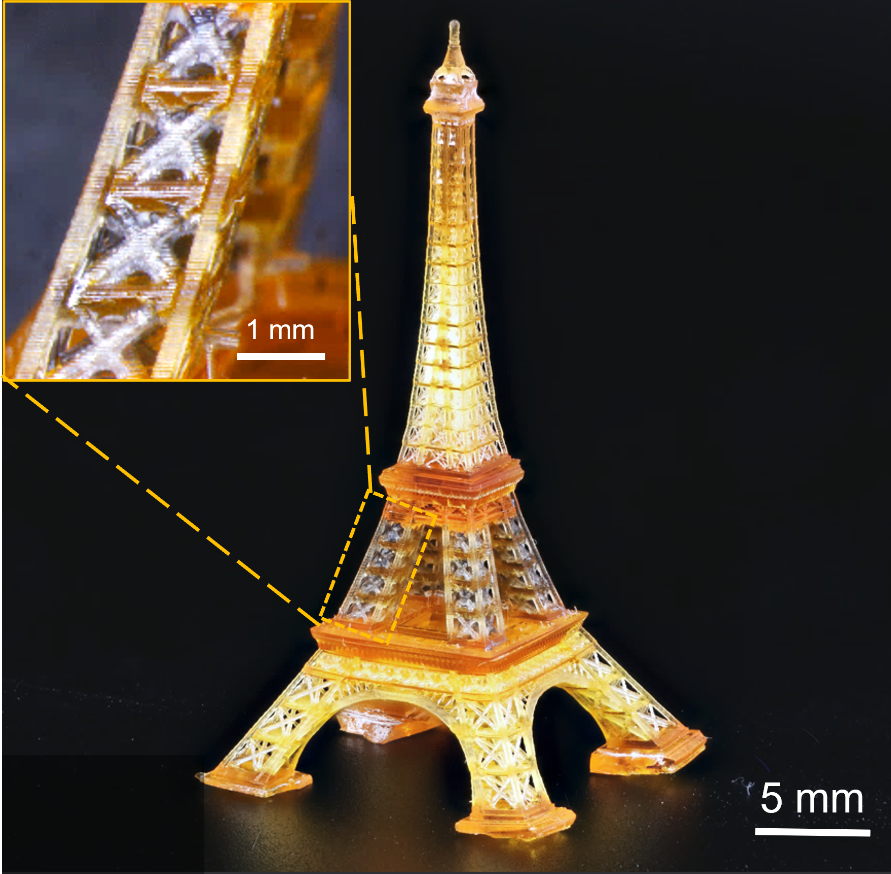
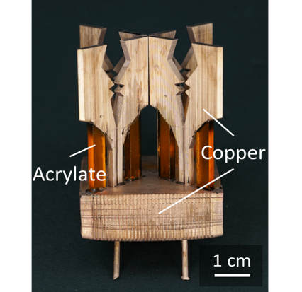
Here we actively pursue several areas in additive manufacturing science and technology with a focus on end-to-end products: 1) Additive manufacturing techniques of multi-scale architectures. We develop additive manufacturing techniques capable of assembling microscale features over large areas (from micro-meter to meter level); novel processes that introduce mesoscale control of features over 3D topology: e.g., 3D alignment of nano-scale inclusions. 2) High-speed multi-material additive manufacturing innovations capable of rapid assembly of electronic, conductive and dielectric materials into 3D electro-mechanical systems. 3) Device integration, packaging and deployment.
Thrust 2: Computational and Artificial Intelligence Design for Metamaterials
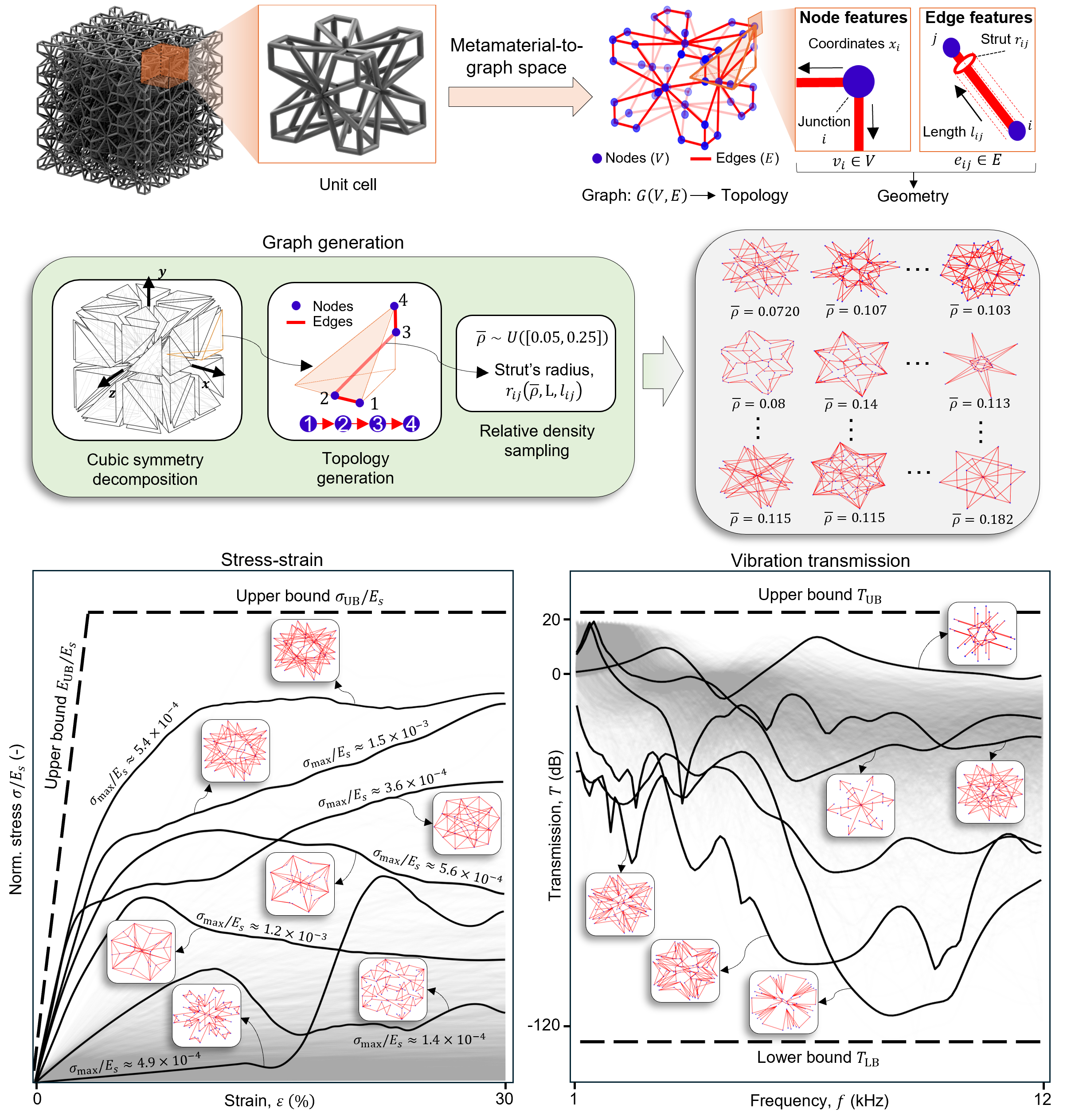
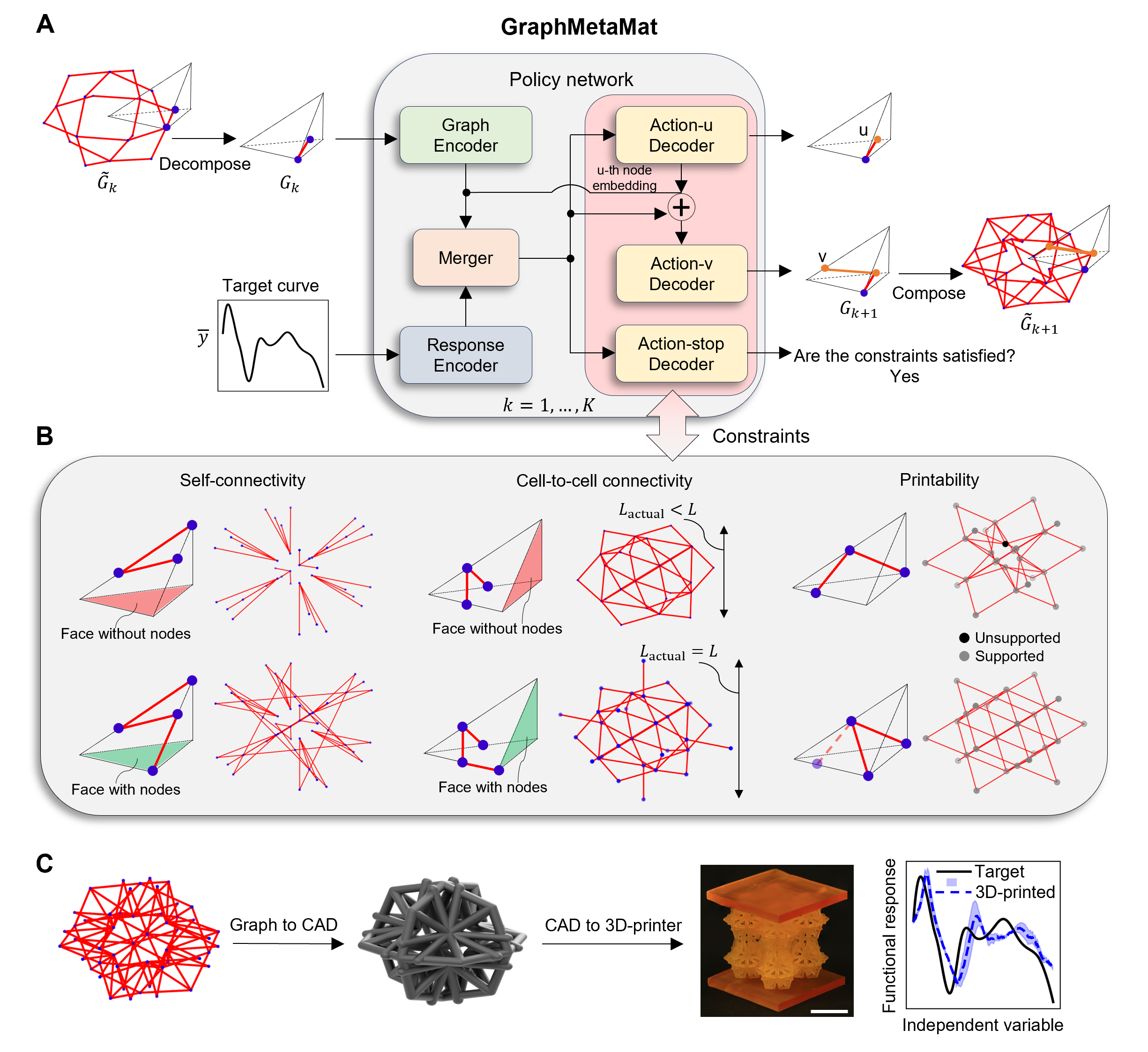
Most commonly, material properties (such as density, strength, toughness, stiffness, thermal, piezoelectricity, ferroelectricity) are highly coupled in natural and man-made materials. The aim of this research is to capitalize the unique benefits design of artificial 3D architectures spanning multiple hierarchical levels to create new materials that possess designed behaviors and properties. This area of research exploits the intersection of artificial intelligent design, mechanics, and computations and machine learning to design new materials and devices.
Thrust 3: Electronic and Multi-functional Materials for Robotics, Sensors and Energy Storage Devices (piezoelectric, dielectric and conductive materials)
Efforts will be focused on the following areas: 1) Biodegradable tunable microlattices for accelerated cell growth and wound healing, tissue ablation and ultrasound detection. 2) Functionally graded 3D material with biomolecules for biosecurity and countermeasures. 3) Micro-actuators and integrated robots with high force and displacement output and large bandwidth. 4) Smart materials for novel air and underwater transducers for integrated self-sensing.